Lecture Notes and Handouts
- Handout 1 [PDF]: Introduction to the course and to microelectronics.
- Handout 2 [PDF]: Basic semiconductor physics, electrons and holes in semiconductors, generation and recombination, doping in semiconductors, N-doped and P-doped semiconductors.
- Handout 3 [PDF]: Electron and hole transport in semiconductors, drift and diffusion, mobility and diffusivity, electron and hole current densities, Einstein relations, carrier densities in thermal equilibrium.
- Handout 4 [PDF]: Recombination and generation in semiconductors, majority and minority carriers, Shockley equations, quasi-neutrality.
- Handout 5 [PDF]: PN junctions in thermal equilibrium, built-in potential, depletion regions, balance between drift and diffusion current densities.
- Handout 6 [PDF]: Biased PN junctions, forward and reverse biased PN junctions, carrier distributions and current densities in forward and reverse bias.
- Handout 7a; Handout 7b [PDF]: Small signal models of PN diodes, depletion and diffusion capacitances, light emitting PN diodes (LEDs). Photovoltaics and solar cells, light generation and carrier transport, quantum efficiency, power conversion efficiency, practical solar cells.
- Handout 8a; Handout 8b [PDF]: Metal oxide semiconductor (MOS) capacitors, equilibrium, flatband, accumulation, depletion, and inversion, charge storage and capacitance of the MOS structure, small signal models, NMOS and PMOS structures.
- Handout 9a; Handout 9b [PDF]: MOS field effect transistors (FETs), regimes of operation; cut-off, linear (triode), and saturation, MOS current vs voltage relations, backgate effect, velocity saturation effects, and breakdown.
- Handout 10 [PDF]: Large signal and small signal models for MOS transistors, simple MOSFET amplifier and logic circuits, low frequency and high frequency small signal circuit models of MOSFETs, capacitances in small signal models.
- Handout 11 [PDF]: Single Stage FET amplifiers; general amplifier concepts and two-port models, open circuit voltage gain and short circuit current gain, input and output resistances, common source (CS).
- Handout 12 [PDF]: Single Stage FET amplifiers; common gate (CG) amplifier circuits, common drain (CD) amplifier circuits.
- Handout 13 [PDF]: Biasing and loading single stage FET amplifiers, active loads and active biasing schemes, cascode loads.
- Handout 14 [PDF]: FET current and voltage sources/sinks, FET current mirrors, cascode designs, Wilson current mirror, active biasing schemes.
- Handout 15 [PDF]: Multistage FET amplifiers, cascade design, cascode design, active biasing schemes.
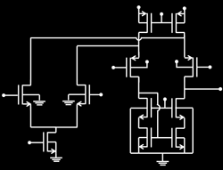
- Handout 16 [PDF]: FET differential amplifiers, common-mode and difference-mode inputs and outputs, single-ended and double-ended outputs, large signal and small signal analysis of differential amplifiers.
- Handout 17 [PDF]: Differential amplifiers with current mirrors, large signal and small signal analysis, difference-mode and common-gain, output resistance, cascode differential amplifiers with cascode current mirrors.
- Handout 18a; Handout 18b [PDF]: Bipolar junction transistors, regimes of operation, Ebers-Moll model, small signal models, NPN and PNP devices.
- Handout 19 [PDF]: High frequency small circuit analysis of FET circuits, high frequency analysis of common source amplifiers, frequency dependent voltage and current gains, Miller effect and the Miller capacitance, transition frequency, and the ultimate limits on the high frequency performance of FETs.
- Handout 20 [PDF]: High frequency amplitude and phase response of amplifiers, gain margin and phase margin, feedback and stability, and frequency compensation.
- Handout 21 [PDF]: Advanced circuit techniques, method of open circuit time constants, telescopic cascode and folded cascode designs, folded cascode differential amplifiers.
- Handout 22 [PDF]: Advanced circuit techniques in communications, RF mixers and modulators, single and double balanced mixers, A/D and D/A converters, sample and hold circuits.
- Handout 23 [PDF]: CMOS logic gates, CMOS inverter, digital levels and noise margins, charging and discharging dynamics, rise times and fall times, and power dissipation.
- Handout 24 [PDF]: Static CMOS logic, CMOS NAND gate, CMOS NOR gate, more complex logic gates, FET scaling, CMOS transmission gate, CMOS latches and flip-flops, CMOS memory, SRAM and DRAM.
- Handout 25 [PDF]: Subthreshold FET operation, strong inversion and weak inversion, inverse subthreshold slope of FETs, subthreshold circuits.
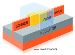
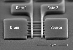
- Handout 26 [PDF]: Nano-scale FETs, FET scaling to small dimensions, short channel effects, current technology trends, FinFETs.
- Handout 27 [PDF]: New physics at the nano scales, quantum effects, quantum transport, new materials; graphene and nanotubes, and emerging technologies.


